AnyLayer PCB |
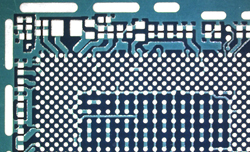
| These are PCBs that enable free connection between all layers combining laser technology and filled plating technology that allows ultra-fine processing. With the higher degree of design freedom and higher-density wiring, these PCBs are ideal for the needs of downsizing and thinning of smartphones and other high performance devices. |
 |
|
| |
Features |
- AnyLayer PCBs with Laser Via and Filled Plating on each layer
- Thinner 0.4mm pitch CSP by AnyLayer interconnection supported
- Mass-production of 10-layer M-VIA Ⅲ (AnyLayer PCBs) for mobile devices
|
| |
| Cross section |
Stackup |
 |
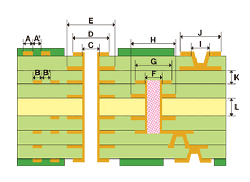 |
| AnyLayer PCB (M-VIA Ⅲ) |
10-layer M-VIA Ⅲ |
|
| |