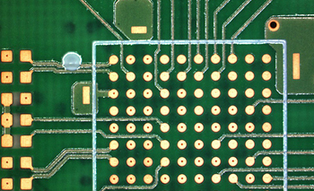
HDI PCB (M-VIA Ⅰ/Ⅱ) |
| These are multi-layer PCBs in which layers are piled up one by one using laser technology and plating technology after forming a conductor pattern on an insulating layer. Because wiring is possible on the connection part of each layer, this method achieves higher density and higher integration than ordinary multi-layer through-hole PCBs. They are used for devices that require high-density wiring in a limited space. |
 |
|
| |
Features |
- HDI PCBs with Staggered Via and Stacked Via
- Any combination with Laser Via, IVH or Plated Through Hole is possible
|
| |
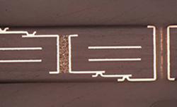
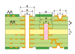
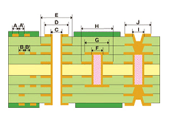
Cross section |
 |
 |
| M-VIA I (Staggered Via) |
M-VIA II (Stack Via) |
|
| |
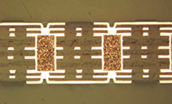
Stackup |
 |
 |
| M-VIA I (Staggered Via) |
M-VIA II (Stack Via) |
|