Embedded Devices PCB |
Small mobile devices feature an increasing number of passive components that require a higher-density installation. Unfortunately the surface mounting area of conventional surface-mount technology (two-dimensional implementation) is unable to support these components. That is why the three-dimensional implementation using embedded PCB technology was proposed.
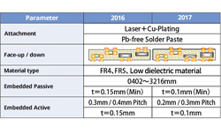
we independently developed a connection process using laser via and plating in addition to a bonding process using solder materials, and has a track record of mass production with both processes. |
 |
|
| |
Features |
- Reduction of the surface mount area by embedding chip components (resistance/condenser)
- Improvement of electrical properties by shorter wiring distance between surface-installed ICs and embedded components
- Shorter pitches between components and better heat resistance
enabled by connection between component terminals using laser via and copper plating
|
| |
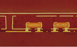
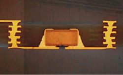
Cross section |
 |
 |
| Plating connection |
soldered joint (6-layer mass produced products) |
|
| |
Development roadmap |
|